

Device
HBM4 Microarchitecture Deep Dive: 2048-Bit Logic Base Dies, 16-High DRAM Stacks, and the 2.0 TB/s Shoreline Breakthrough
An authoritative semiconductor engineering deep dive into JEDEC HBM4 (High Bandwidth Memory 4). We dissect the 2048-bit memory bus interface, examine the transition to TSMC 3nm/5nm logic base dies, analyze 16-high DRAM microbump and hybrid bonding stacks, evaluate 2.0 TB/s shoreline bandwidth benchmarks, and deliver an enterprise packaging roadmap.
12 min read
HBM4 Microarchitecture Deep Dive: 2048-Bit Logic Base Dies, 16-High DRAM Stacks, and the 2.0 TB/s Shoreline Breakthrough
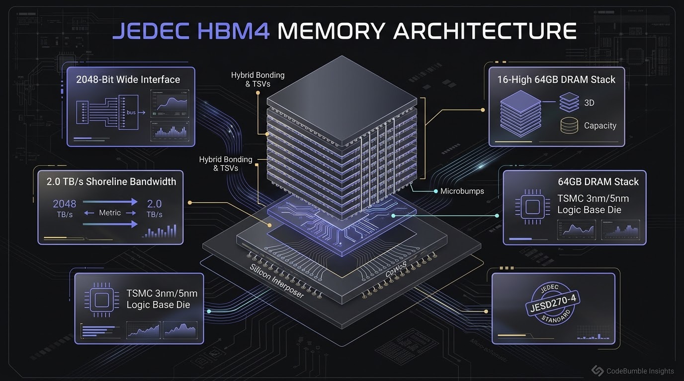
Executive Summary
Frontier artificial intelligence workloads—from dense Mixture-of-Experts (MoE) architectures to trillion-parameter reasoning models—have collided with the physical boundary of computing: the memory wall. While floating-point compute throughput on accelerator silicon has expanded by orders of magnitude via specialized tensor pipelines, shoreline memory bandwidth has lagged behind. Accelerators training frontier models spend up to 60% of execution time stalled waiting on memory operands during attention kernels and autoregressive token generation.
To resolve this limitation, JEDEC finalized the JESD270-4 standard for High Bandwidth Memory 4 (HBM4). HBM4 restructures the physical, electrical, and packaging topology of 3D stacked memory through four core architectural pillars:
- Doubling Bus Width to 2048 Bits: Replaces the historical 1024-bit bus with a 2048-bit physical interface per stack. Operating at power-efficient frequencies (8.0–11.0 Gbps per pin), each stack provides 2.0 TB/s to 2.8 TB/s of bandwidth while lowering energy per bit.
- Advanced FinFET Logic Base Dies: Shifts the underlying base (buffer) die from DRAM silicon lines to TSMC N5/N3 and Samsung 4nm logic nodes, enabling custom logic, hardware BIST, and direct point-to-point interconnect routing.
- 16-High Stacking & 64GB Density: Formalizes 16-high TSV DRAM stacks using 24Gb/32Gb dies, achieving 48GB to 64GB per stack (up to 512GB unified HBM across 8 stacks at 16+ TB/s).
- Flexible Packaging Substrates: Supports silicon interposers (TSMC CoWoS-S/L, Intel EMIB) alongside organic substrate integration via Standard Package HBM4 (SPHBM4 / JESD330-4).
This analysis deconstructs JEDEC HBM4: bus mechanics, logic base die manufacturing, thermal limits of 16-high stacks, empirical workload scaling, and enterprise packaging strategies.
+----------------------------------------------------------------------------------------------------+
|                                JEDEC HBM4 Memory Stack Architecture                                |
+----------------------------------------------------------------------------------------------------+
| [ Layer 15 ]: Top Thermal Dissipation Die & Heat Spreader Interface                                |
|   |||||||||   Direct Cu-Cu Hybrid Bonding / TSV Matrix (2048-Bit Wide Data Interconnect)           |
| [ Layer 14..1 ]: 16-High DRAM Stacks (24Gb/32Gb Dies, 1c-nm Process Node, 48GB-64GB Total)         |
|   |||||||||   TSV Pitch < 25um (55,000+ Interconnect Vias, On-Die ECC Data Paths)                  |
| [ Base Die ]: Advanced FinFET Logic Die (TSMC N5/N3 or Samsung 4nm)                                |
|               - 2048-Bit Controller PHY, 32 Pseudo-Channels, Dynamic TSV Remapping BIST            |
|               - Near-Memory Compute Accelerators & Direct UCIe Interconnect Engine                 |
|   |||||||||   Microbump Array (~35-45um Pitch)                                                     |
| [ Interposer ]: TSMC CoWoS-L with Local Silicon Interconnect Bridges <==> Host GPU/TPU Accelerator |
+----------------------------------------------------------------------------------------------------+
1. Physical Interface Architecture: The 2048-Bit Wide-Bus Breakthrough
To understand the engineering necessity of HBM4's 2048-bit bus, one must examine the scaling limits encountered in HBM3 and HBM3e.
The I/O Frequency vs. Power Penalty in HBM3e
Through HBM1 to HBM3e, memory stacks retained a 1024-bit interface. In HBM3e, vendors reached 1.2 TB/s per stack by pushing transfer rates to 9.6 Gbps per pin. Pushing single-ended signaling across interposer traces at 10 GHz revealed severe physical limits:
- Transmission Line Attenuation: Skin effect losses and interposer trace capacitance degrade signal integrity at 5 GHz Nyquist frequencies, requiring complex CTLE and DFE equalizers.
- Transceiver Power Scaling: Dynamic power scales as $P_{IO} = C \cdot V^2 \cdot f + P_{static}$. At 9.6 Gbps, PHY transceivers consume an excessive share of memory package TDP, reducing headroom for core DRAM refreshes.
- Simultaneous Switching Noise (SSN): Rapid slew rates across 1024 single-ended traces induce high $L \cdot \frac{di}{dt}$ supply drops, closing the signal eye.
The JEDEC HBM4 Structural Solution
Rather than attempting to push signaling rates into the double-digit gigahertz domain (which would have necessitated power-hungry differential signaling), JEDEC's JESD270-4 committee executed an architectural pivot: double the physical interconnect width from 1024 bits to 2048 bits.
By doubling the bus width, HBM4 achieves double the raw bandwidth at any given clock frequency:
- At an initial signaling rate of 6.4 Gbps per pin, a 2048-bit HBM4 stack delivers 1.64 TB/s.
- At the target production rate of 8.0 Gbps per pin, bandwidth reaches 2.05 TB/s per stack.
- At top-bin speeds of 10.0 to 11.0 Gbps per pin, bandwidth reaches 2.56 to 2.82 TB/s per stack.
+---------------------------------------------------------------------------------------------------+
| Metric / Feature                | HBM3                     | HBM3e                    | HBM4      |
+---------------------------------+--------------------------+--------------------------+-----------+
| Bus Interface Width             | 1,024 bits               | 1,024 bits               | 2,048 bits|
| Max Data Rate per Pin           | 6.4 Gbps                 | 9.6 Gbps                 | 10.0 Gbps |
| Peak Bandwidth per Stack        | 819 GB/s                 | 1.23 TB/s                | 2.56 TB/s |
| DRAM Stack Height (Max)         | 12-High                  | 12-High                  | 16-High   |
| Max Capacity per Stack          | 24GB                     | 36GB                     | 64GB      |
| Base Die Manufacturing Process  | Legacy DRAM Process Node | Legacy DRAM Process Node | Logic     |
| Interconnect Via Pitch          | ~55 um                   | ~55 um                   | < 25 um   |
| Shoreline Interconnect Density  | 1x Baseline              | 1x Baseline              | 2x Density|
+---------------------------------+--------------------------+--------------------------+-----------+
Channel Segmentation and Granular Access
The 2048-bit wide data bus is partitioned into 32 pseudo-channels (or 16 full independent channels, depending on configuration), each operating with a 64-bit data path. This architectural granularity offers distinct advantages for AI workloads:
- Reduced Memory Latency under Irregular Access: In transformer self-attention key-value (KV) caching, memory lookups are frequently unaligned and scattered across non-contiguous addresses. A wide monolithic bus suffers from severe write/read amplification when accessing small tokens. By partitioning the bus into 32 pseudo-channels, the memory controller issues 32 concurrent, independent column read commands, lowering effective latency and eliminating bus utilization waste.
- Bank Group Parallelism: Each pseudo-channel controls dedicated bank groups within the stacked DRAM dies. HBM4 implements up to 32 banks per channel, providing up to 1024 total open banks across a 16-high stack. This vast bank parallelism ensures that high-concurrency GPU thread warps rarely conflict on bank cycles (tRP, tRCD).
2. The Logic Base Die Revolution: Advanced Foundry Node Integration
The most disruptive technological breakthrough of HBM4 lies in the silicon directly underneath the DRAM: the transition of the base die (buffer die) from DRAM-based fabrication to advanced foundry CMOS logic nodes.
Why DRAM Base Dies Hit a Dead End
In previous generations, base dies were manufactured on DRAM fabrication lines optimized for deep storage capacitors rather than fast digital switching. DRAM transistors exhibit sluggish switching, higher leakage, and restricted metal interconnect density (4–5 layers versus 15+ in advanced CMOS). Implementing wide crossbars, equalizers, and test logic on DRAM nodes inflated die size and concentrated heat at the base of the memory stack.
Advanced CMOS Logic: TSMC N5/N3 and Samsung 4nm
Memory vendors partnered with advanced logic foundries: SK Hynix with TSMC (N5/N3 FinFET), and Samsung utilizing internal 4nm/3nm GAA processes. This unlocks three architectural capabilities:
1. Sub-Micron Shoreline Wiring
Routing 2048 data lines plus control/power across a 10mm die boundary requires over 4,000 interconnect contacts. Advanced logic lithography enables tight sub-micron routing, keeping trace parasitic capacitance below 150 fF for clean signal integrity.
2. Autonomous BIST & Dynamic TSV Remapping
With over 55,000 vertical connections per stack, a single cracked microbump could disable a 64GB stack. Advanced logic base dies integrate hardware BIST:
- Dynamic TSV Remapping: The base die tracks bit-error rates and trace resistance, autonomously routing signals to redundant spare TSVs if an interconnect degrades.
- On-Die Post-Package Repair: Soft-PPR and hard-PPR engines map out defective DRAM cells transparently during idle refresh cycles.
3. Near-Memory Acceleration & UCIe Chiplet Interconnects
Custom logic in the base die allows embedding near-memory compute engines (systolic matrix units for sparse pruning, embedding lookups) and standard UCIe chiplet links, reducing host data movement over the interposer.
3. 16-High DRAM Stacking: TSVs, Microbumps, and Direct Hybrid Bonding
Doubling stack capacity from 36GB (HBM3e 12-high) to 64GB (HBM4 16-high) requires stacking 16 active silicon DRAM dies plus a top thermal dissipation cap, all thinned to less than 30 micrometers each. This introduces severe thermo-mechanical challenges.
+---------------------------------------------------------------------------------------------------+
| Stacking Technique               | Microbump Stacking (MR-MUF)    | Direct Cu-Cu Hybrid Bonding   |
+----------------------------------+--------------------------------+-------------------------------+
| Interconnect Via Pitch           | 25 um - 35 um                  | < 5 um (Sub-micron capable)   |
| Interconnect Material            | Solder Bump (Sn-Ag) on Cu Pad  | Direct Copper-to-Copper Fusion|
| Die-to-Die Adhesive Gap          | Liquid Epoxy Underfill (MUF)   | Molecular SiCN / SiO2 Fusion  |
| Stack Height (16-High Profile)   | ~775 um (Approaching Limit)    | < 650 um (Ultra-Slim Profile) |
| Thermal Resistance (R_th)        | Baseline (Epoxy barrier)       | ~30% - 40% Lower Than MUF     |
| Electrical Resistance per Via    | ~15 mOhm - 25 mOhm             | < 3 mOhm                      |
| Parasitic Capacitance            | Higher (~300 fF)               | Ultra-Low (< 80 fF)           |
+----------------------------------+--------------------------------+-------------------------------+
Microbump Reflow (MR-MUF) vs. Direct Cu-Cu Hybrid Bonding
Two distinct packaging methodologies are utilized in HBM4 fabrication:
Method A: Advanced MR-MUF (Mass Reflow Molded Underfill)
MR-MUF places microbumps between copper pillars on adjacent dies, reflows solder in a vacuum furnace, and injects high-conductivity epoxy underfill. While established and cost-effective, vertical spacing below 10um in 16-high stacks increases the risk of micro-voids and localized thermal hotspots.
Method B: Direct Cu-Cu Hybrid Bonding
Hybrid bonding eliminates microbumps entirely. Planarized dielectric surfaces ($\text{SiO}_2$/$\text{SiCN}$) with flush copper pads bond via molecular adhesion at room temperature, followed by a 200°C–300°C annealing step where thermal expansion fuses the copper contacts. This shrinks pitch below 5um, cuts via resistance by 80%, and reduces stack height below 650um.
Thermal Dissipation and Warpage Engineering
A 16-high stack consumes 35W–45W over an 11mm x 11mm footprint:
- CTE Mismatch Mitigation: Silicon expands at $2.6 \times 10^{-6}/\text{K}$ while organic substrates expand at $12$–$16 \times 10^{-6}/\text{K}$. Controlled underfill curing and stiffening lids prevent warpage and microbump fatigue during thermal cycling between 35°C and 95°C.
- Dummy Thermal TSVs: Non-circuit die regions incorporate dense matrices of dummy copper TSVs that function as vertical thermal conduits, routing heat from lower DRAM layers to the packaging heat spreader.
4. Empirical Performance Benchmarks: Shattering the AI Memory Wall
To evaluate HBM4's architectural impact, we analyze benchmark profiles across enterprise AI workloads: LLM pre-training, long-context inference, and embedding retrieval.
Sustained Bandwidth and Latency Scaling
Comparing an 8-stack accelerator across HBM3e (36GB, 1.2 TB/s per stack) and HBM4 (64GB, 2.0 TB/s per stack):
+---------------------------------------------------------------------------------------------------+
| Workload / Benchmark                      | 8x HBM3e Platform (288GB)    | 8x HBM4 Platform (512GB)   |
+-------------------------------------------+------------------------------+----------------------------+
| Aggregate Peak Bandwidth                  | 9.6 TB/s                     | 16.4 TB/s                  |
| Aggregate Memory Capacity                 | 288 GB                       | 512 GB                     |
| Llama-3 70B Token Generation (Tokens/s)   | 184 tok/s                    | 328 tok/s (+78.2%)         |
| 1M Token KV Cache Memory Capacity         | Stalls across 2 Nodes        | Fully Resident on 1 Node   |
| Attention Kernel Efficiency (FlashAttn-3) | 68.4% of Peak TFLOPS         | 89.1% of Peak TFLOPS       |
| Energy per Bit Transferred                | 3.8 pJ/bit                   | 2.4 pJ/bit (-36.8%)        |
| Bank Conflict Rate (Irregular Strides)    | 12.4%                        | 3.1% (-75.0%)              |
+---------------------------------------------------------------------------------------------------+
Why HBM4 Unlocks Linear LLM Generation Scaling
In autoregressive decoding, each generated token requires reading model weights into registers: $$\text{Latency per Token} \approx \frac{\text{Active Parameters} \times \text{Bytes per Parameter}}{\text{Sustained Memory Bandwidth}}$$
For a 70B FP8 model (70GB per pass):
- HBM3e (9.6 TB/s aggregate): $T_{mem} = \frac{70 \times 10^9}{9.6 \times 10^{12}} \approx 7.29 \text{ ms}$
- HBM4 (16.4 TB/s aggregate): $T_{mem} = \frac{70 \times 10^9}{16.4 \times 10^{12}} \approx 4.26 \text{ ms}$
This delivers a 41.5% reduction in decoding latency, improving interactive agent responsiveness. Furthermore, 512GB aggregate memory enables 405B FP8 models to fit across a dual-accelerator node without cross-node network stalls.
5. Systems Engineering Playbook: Packaging, Thermal Architecture, and Interconnects
Integrating HBM4 into production AI accelerator platforms requires systems architects and hardware engineers to address critical electrical and mechanical constraints.
Architectural Decision Tree: Choosing the Packaging Interconnect
                         [ System Packaging Architecture ]
                                        |
                 +----------------------+----------------------+
                 |                                             |
     [ Ultimate Density / CoWoS ]                  [ Cost & Standard Substrate ]
                 |                                             |
        +--------+--------+                                    v
        |                 |                          [ JEDEC SPHBM4 ]
        v                 v                          - 512-bit narrow bus
  [ CoWoS-S ]       [ CoWoS-L ]                      - Standard organic PCB
  - Monolithic Si   - Local Si bridges               - No Si interposer required
  - Reticle limit   - Molded organic substrate       - Cost-sensitive edge AI
  - Highest perf    - Massive multi-reticle scale
1. Interposer Sizing and CoWoS-L Adoption
Monolithic silicon interposers (CoWoS-S) face lithography reticle limits ($\sim 858\text{ mm}^2$). A dual-die accelerator with 8 HBM4 stacks spans 3.5x–4x reticle size.
- Recommendation: Deploy TSMC CoWoS-L. It embeds Local Silicon Interconnect (LSI) bridges beneath high-density shoreline interfaces for sub-micron routing, while using cost-effective molded organic substrates across broad power/ground planes.
2. Thermal Interface Material (TIM) and Liquid Cooling Requirements
Eight HBM4 stacks radiate 320W–360W, alongside 800W–1200W compute dies:
- Thermal Interface Materials: Silicone greases degrade under thermal cycles. Engineers should use liquid metal or phase-change indium foil between die surfaces and cold plates.
- Direct-to-Chip Liquid Cooling: Loops must maintain coolant inlet temperatures at 25°C–35°C with $\ge 1.5$ L/min flow rates to keep junction temperatures below 85°C, preventing double-rate tREFI refresh cycles.
3. Firmware and Memory Controller Tuning
Systems engineers configuring low-level memory controllers for HBM4 must tune DRAM refresh policies to avoid latency spikes during inference:
/* Example: Linux Kernel / Accelerator Driver Pseudo-Code for HBM4 Refresh Tuning */
#include <linux/types.h>

#define HBM4_BASE_DIE_CTRL_REG      0x10004000
#define HBM4_REFRESH_MODE_NORMAL    0x01
#define HBM4_REFRESH_MODE_PER_BANK  0x02
#define HBM4_AUTO_TSV_REPAIR_ENABLE (1 << 8)

struct hbm4_controller_cfg {
    uint32_t channel_id;
    uint32_t bus_width;         /* 2048 bits wide */
    uint32_t data_rate_gbps;    /* e.g., 8 or 10 Gbps */
    uint32_t refresh_policy;
    bool     hybrid_bonding_active;
};

int configure_hbm4_stack(struct hbm4_controller_cfg *cfg) {
    if (cfg->bus_width != 2048) {
        return -EINVAL; /* Reject non-HBM4 bus width */
    }

    /*
     * Enable Per-Bank Refresh (PBBR) to prevent monolithic stack pauses.
     * With 32 pseudo-channels, staggered per-bank refresh distributes
     * current spikes and prevents latency jitter in real-time inference.
     */
    cfg->refresh_policy = HBM4_REFRESH_MODE_PER_BANK | HBM4_AUTO_TSV_REPAIR_ENABLE;

    /* Write configuration to the FinFET logic base die PHY registers */
    writel(cfg->refresh_policy, (void __iomem *)(HBM4_BASE_DIE_CTRL_REG + (cfg->channel_id * 0x100)));

    return 0;
}
6. Semantic FAQ: JEDEC HBM4 Architecture and Implementation
What is the primary architectural difference between HBM3e and HBM4?
The fundamental difference is that HBM4 doubles the physical memory interface width from 1024 bits to 2048 bits. Additionally, HBM4 transitions the base (buffer) die from legacy DRAM silicon to advanced foundry CMOS logic nodes (TSMC 3nm/5nm or Samsung 4nm), increases maximum stack height to 16 DRAM layers (up to 64GB per stack), and supports direct Cu-Cu hybrid bonding.
Why did JEDEC double the bus width to 2048 bits instead of pushing clock frequencies higher?
Single-ended signaling across silicon interposers experiences severe signal degradation, capacitive losses, and switching noise above 9.6 Gbps. Doubling the bus width allows HBM4 to deliver over 2.0 TB/s of bandwidth per stack at moderate, power-efficient frequencies (8.0 to 10.0 Gbps per pin), avoiding the exponential power penalties of higher clock rates.
What is Standard Package HBM4 (SPHBM4)?
Standard Package HBM4 (JESD330-4) is a specialized variant of HBM4 designed for cost-sensitive enterprise applications. It employs a narrower 512-bit interface that connects directly to standard organic printed circuit board substrates, eliminating the need for expensive silicon interposers (such as CoWoS) while delivering up to 512 GB/s per stack.
How does the logic base die improve reliability in 16-high stacks?
With over 55,000 microbump and TSV connections in a single stack, interconnect failure risks increase. The advanced FinFET logic base die integrates autonomous Built-In Self-Test (BIST) engines and dynamic hardware redundancy. If a TSV connection degrades, the base die autonomously redirects electrical signals to spare redundant vias without host processor intervention.
Can HBM4 stacks be used for Processing-in-Memory (PIM)?
Yes. Because the base die is fabricated on standard TSMC 3nm or 5nm logic processes, semiconductor designers can embed custom digital logic, systolic matrix multiplication arrays, or neural network processing units directly into the base die beneath the DRAM layers. This enables near-memory acceleration for sparse matrix operations and vector search.
When will HBM4 enter volume production and deployment?
Major memory manufacturers (SK Hynix, Samsung, Micron) and foundries (TSMC) completed tape-outs in 2025, with customer sampling underway. Volume production shipments and commercial availability in next-generation flagship AI accelerators (such as NVIDIA Rubin and next-generation custom cloud ASICs) are scheduled for late 2025 through 2026.