

Device
Inside MediaTek Dimensity 9400: TSMC 3nm Floorplan, Cortex-X925 All-Big-Core Silicon, and 50 TOPS Agentic AI
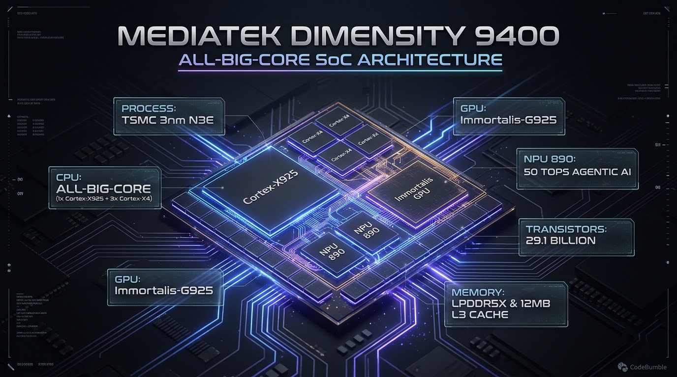
MediaTek's Dimensity 9400 breaks conventional mobile processor design by eliminating little efficiency cores in favor of an aggressive All-Big-Core architecture built on TSMC's 2nd-generation 3nm (N3E) node. Packing 29.1 billion transistors across an estimated 125–130 mm² die, the SoC combines a 3.62GHz ARM Cortex-X925 prime core with 2MB of private L2 cache, three Cortex-X4 performance cores, four Cortex-A720 units, and the 50 TOPS NPU 890. This deep systems engineering teardown analyzes its physical floorplan, cache hierarchy, memory bandwidth scaling, and thermal throttling mitigations.
13 min read
Inside MediaTek Dimensity 9400: TSMC 3nm Floorplan, Cortex-X925 All-Big-Core Silicon, and 50 TOPS Agentic AI
Executive Summary
The semiconductor industry is witnessing an aggressive divergence in mobile system-on-chip (SoC) microarchitecture. While mobile processors historically relied on ARM's big.LITTLE heterogeneous topology—pairing high-power performance cores with low-power efficiency cores to preserve battery life—MediaTek radically disrupted this design paradigm. Building on the foundation established by the Dimensity 9300, the flagship MediaTek Dimensity 9400 (MT6991Z) eliminates "LITTLE" efficiency cores entirely, deploying an uncompromising All-Big-Core architecture manufactured on TSMC's second-generation 3nm process node (N3E).
Recent physical teardowns and silicon floorplan analyses from TechInsights reveal the exact engineering compromises and transistor density breakthroughs required to execute an all-big-core design on a commercial smartphone footprint. Packing 29.1 billion transistors into an estimated 125–130 mm² die, the Dimensity 9400 integrates ARM's latest Cortex-X925 prime core clocked at 3.62GHz with 2MB of private L2 cache, supported by three Cortex-X4 performance cores at 3.3GHz, four Cortex-A720 cores at 2.4GHz, and a massive 12MB unified L3 cache paired with a 10MB System-Level Cache (SLC).
Beyond raw scalar compute, the Dimensity 9400 introduces major architectural revisions to its acceleration subsystems: the 12-core ARM Immortalis-G925 GPU delivering desktop-class hardware ray tracing, an 8th-generation MediaTek NPU 890 delivering 50 TOPS of on-device agentic AI compute, and the industry's first production memory controller supporting LPDDR5X-10667 RAM at 85.3 GB/s bandwidth.
This technical deep dive explores the microarchitecture of the MediaTek Dimensity 9400. We examine the physical silicon floorplan, analyze the thermodynamic rationale behind abandoning efficiency cores, evaluate cache and memory hierarchy scaling, benchmark IPC and power curves against Qualcomm's Snapdragon 8 Elite and Apple's A18 Pro, and provide an engineering optimization playbook for developers profiling on-device workloads under Android.
1. The Death of the Little Core: Architectural Rationale for All-Big-Core
1.1 The Race-to-Sleep Thermodynamic Hypothesis
For over a decade, mobile processors relied on small efficiency cores (Cortex-A55 / Cortex-A520) for background tasks, assuming minimal static leakage yielded the lowest battery draw.
However, as process nodes scaled past 7nm down to TSMC's 3nm N3E, two physical realities upended this assumption:
- Dynamic Energy vs. Execution Duration ($E = P \times t$): While a small efficiency core draws lower peak power (e.g., 200mW), its narrow 2-wide execution pipeline requires a significantly longer duration ($t$) to complete instructions. In contrast, an aggressive out-of-order performance core (like the Cortex-A720) operates at higher instantaneous power (e.g., 600mW) but completes the task in a fraction of the time, allowing the CPU to power-gate back to zero idle voltage almost instantaneously. This phenomenon—known as "race to sleep"—often results in lower total integrated energy per operation for bursty mobile workloads.
- Instruction Footprint Inflation in Modern OS Runtimes: Modern Android runtimes (ART, Play Services, JavaScript engines) execute heavy instruction sequences that exceed the small caches of efficiency cores, causing pipeline stalls and wasted leakage during memory fetches.
+----------------------------------------------------------------------------------------------------+
|                         Race-to-Sleep Energy Comparison: Big vs. Little Core                       |
+----------------------------------------------------------------------------------------------------+
|                                                                                                    |
|  CONVENTIONAL EFFICIENCY CORE (Cortex-A520):                                                       |
|  Power [mW]                                                                                        |
|   400 |                                                                                            |
|   200 |+-------------------------------------------------------------+                             |
|     0 +--------------------------------------------------------------+-------> Time [ms]           |
|       |<----------------- Long Execution Duration (120ms) ----------->|                            |
|       Integrated Energy = 200mW * 120ms = 24.0 mJ                                                  |
|                                                                                                    |
|  ALL-BIG-CORE PERFORMANCE UNIT (Cortex-A720 @ Tuned Operating Point):                              |
|  Power [mW]                                                                                        |
|   600 |+------------------+                                                                        |
|   200 ||                  | (Instant Power-Gate to Sleep)                                          |
|     0 ++------------------+--------------------------------------------------> Time [ms]           |
|       |<-- 25ms Burst --->|                                                                        |
|       Integrated Energy = 600mW * 25ms = 15.0 mJ  [ 37.5% Energy Reduction ]                       |
|                                                                                                    |
+----------------------------------------------------------------------------------------------------+
1.2 Voltage/Frequency Curve Optimization
Without little cores, MediaTek avoids routing power rails across three distinct microarchitectures. The four Cortex-A720 cores operate across an ultra-wide V/F curve: running at 0.65V–0.75V (800MHz–1.5GHz) for background tasks with near-idle draw, scaling up to 1.05V (2.4GHz) for sustained multi-threaded compute.
2. Microarchitecture & TSMC N3E Silicon Floorplan Analysis
2.1 Physical Floorplan and Transistor Budget
TechInsights' structural teardown of the MT6991Z silicon reveals a total die size between 125 mm² and 130 mm², housing 29.1 billion transistors fabricated on TSMC's 3nm N3E node. This represents one of the largest and most complex monolithic smartphone dies ever brought to mass production, comparable in area to Qualcomm's Snapdragon 8 Elite (~128 mm²) and Apple's A18 Pro (~110 mm²).
The physical silicon budget allocates die space across four major functional zones:
+----------------------------------------------------------------------------------------------------+
|                       MediaTek Dimensity 9400 Physical Silicon Floorplan                           |
+----------------------------------------------------------------------------------------------------+
|                                                                                                    |
|  +-------------------------------------+  +-----------------------------------------------------+  |
|  | CPU CLUSTER (~22.0 mm² Total)       |  | GPU CLUSTER (~22.5 mm² Total)                       |  |
|  |                                     |  |                                                     |  |
|  |  +-------------------------------+  |  |  ARM Immortalis-G925 MC12 (12 Shader Cores)         |  |
|  |  | 1x Cortex-X925 @ 3.62GHz      |  |  |  - Dedicated Hardware Ray Tracing Units             |  |
|  |  | (3.2 mm² area, 2MB L2 Cache)   |  |  |  - 5th Gen Valhall Architecture                     |  |
|  |  +-------------------------------+  |  |  - Dynamic Micro-Tile Tiling Engine                |  |
|  |                                     |  +-----------------------------------------------------+  |
|  |  +-------------------------------+  |                                                           |
|  |  | 3x Cortex-X4 @ 3.3GHz         |  |  +-----------------------------------------------------+  |
|  |  | (1MB L2 Cache per core)       |  |  | AI ACCELERATION: NPU 890 (~14.5 mm² Total)          |  |
|  |  +-------------------------------+  |  |                                                     |  |
|  |                                     |  |  - 50 TOPS Peak Tensor Compute (FP16 / INT8 / INT4)  |  |
|  |  +-------------------------------+  |  |  - Hardware Generative AI & Diffusion Engine        |  |
|  |  | 4x Cortex-A720 @ 2.4GHz       |  |  |  - On-Device LoRA Training Hardware Unit            |  |
|  |  | (512KB L2 Cache per core)     |  |  +-----------------------------------------------------+  |
|  |  +-------------------------------+  |                                                           |
|  |                                     |  +-----------------------------------------------------+  |
|  |  +-------------------------------+  |  | MEMORY & SYSTEM CACHE (~18.0 mm² Total)             |  |
|  |  | 12MB Shared L3 Cache           |  |  |                                                     |  |
|  |  | + 10MB System-Level Cache (SLC)|  |  |  - 4x 16-bit LPDDR5X-10667 Channels (85.3 GB/s)   |  |
|  |  +-------------------------------+  |  |  - 10MB Low-Power System Cache SRAM Slabs           |  |
|  +-------------------------------------+  +-----------------------------------------------------+  |
|                                                                                                    |
|  +----------------------------------------------------------------------------------------------+  |
|  | PERIPHERALS, 5G SUB-6/mmWAVE MODEM, ISP (Imagiq 1090), AND I/O TILES (~48.0 mm² Total)      |  |
|  +----------------------------------------------------------------------------------------------+  |
|                                                                                                    |
+----------------------------------------------------------------------------------------------------+
2.2 The Cortex-X925 Prime Core: Architectural Evolution
The Cortex-X925 prime core ("Travis") occupies ~3.2 mm² on TSMC N3E (including 2MB L2 cache) and delivers a 35% single-core IPC uplift over Cortex-X4. It features a 10-wide instruction fetch front-end, an out-of-order reorder buffer exceeding 500 entries, dual 256-bit SVE2 vector pipelines, and a doubled 2MB private L2 cache that slashes DRAM fetch latency.
+----------------------------------------------------------------------------------------------------+
|                         Cortex-X925 vs. Cortex-X4 Microarchitectural Metrics                        |
+----------------------------------------------------------------------------------------------------+
| Architectural Parameter   | ARM Cortex-X4 (Dimensity 9300) | ARM Cortex-X925 (Dimensity 9400)      |
+---------------------------+--------------------------------+---------------------------------------+
| Process Node              | TSMC 4nm (N4P)                 | TSMC 3nm (N3E)                        |
| Peak Frequency            | 3.25 GHz                       | 3.626 GHz                             |
| Private L2 Cache          | 1 MB per core                  | 2 MB per core (Doubled)               |
| Instruction Fetch Width   | 8 instructions / cycle         | 10 instructions / cycle               |
| Reorder Buffer (ROB)      | ~384 entries                   | >500 entries                          |
| Vector Extensions         | SVE2 (2x 128-bit)              | SVE2 (2x 256-bit)                     |
| Physical Core Die Area    | ~3.4 mm² (N4P)                 | ~3.2 mm² (N3E with 2MB L2)            |
+---------------------------+--------------------------------+---------------------------------------+
2.3 Shared Memory Subsystem and Cache Topology
To prevent eight aggressive out-of-order cores from starving on memory bandwidth, MediaTek engineered a tiered cache hierarchy:
- L3 Cache: Scaled to 12MB (up from 8MB in prior generations), shared dynamically across all eight CPU cores.
- System-Level Cache (SLC): An additional 10MB SRAM pool buffers memory traffic between the CPU cluster, GPU, NPU, and external DRAM.
- Interconnect: A non-blocking coherent crossbar fabric operating at up to 1.8GHz, capable of delivering over 150 GB/s of internal interconnect throughput.
3. Immortalis-G925 GPU and LPDDR5X-10667 Memory Subsystem
3.1 12-Core ARM Immortalis-G925 Graphics Engine
The Dimensity 9400 integrates the ARM Immortalis-G925 MC12, built on ARM's 5th-generation graphics architecture. Operating 12 shader cores, the GPU delivers up to 40% higher peak performance and 44% greater power efficiency compared to the Immortalis-G720.
The Immortalis-G925 features specialized hardware units for:
- Hardware Ray Tracing: Second-generation ray tracing units deliver a 52% uplift in ray tracing throughput, supporting complex BVH (Bounding Volume Hierarchy) traversals for realistic reflections and global illumination in mobile games.
- Geometry & Micro-Tile Processing: Dynamically sorts and culls hidden primitives prior to fragment shading, slashing memory bandwidth consumption on complex 3D meshes.
- Variable Rate Shading (VRS): Native support for tier-2 VRS allows game engines to allocate shading resources dynamically based on motion vectors and display focus.
3.2 LPDDR5X-10667 Memory Interface
Memory bandwidth is the primary bottleneck for mobile gaming and on-device generative AI models. The Dimensity 9400 is the first smartphone chipset to validate and deploy LPDDR5X-10667 memory:
- Bus Architecture: 4x 16-bit channels (64-bit total bus).
- Clock Frequency: 5,333 MHz (10,667 Mbps data transfer rate).
- Theoretical Peak Bandwidth: 85.33 GB/s, representing a 15% increase over standard 9600 Mbps implementations.
- Impact on AI Inference: Provides the essential memory throughput required to stream large language model (LLM) weights during autoregressive token generation without stalling compute units.
4. MediaTek NPU 890 & Dimensity Agentic AI Engine (DAE)
4.1 50 TOPS Peak Tensor Processing Unit
The MediaTek NPU 890 represents MediaTek's 8th-generation neural processing unit, delivering 50 TOPS (INT8) of peak AI compute. Fabricated on TSMC N3E, the NPU integrates:
- Mixed-Precision Matrix Accelerators: Native support for FP16, BF16, INT8, and hardware-accelerated INT4 quantization, allowing large language models (such as LLaMA-3.2 and DeepSeek-Lite) to execute with 3x lower memory footprints.
- On-Device Speculative Decoding: Dedicated hardware accelerators predict subsequent token sequences concurrently, boosting LLM text generation speeds by up to 40% while reducing total energy consumption.
- Diffusion Transformer (DiT) Hardware Acceleration: Dedicated attention engines speed up on-device image generation (Stable Diffusion) to under 1.5 seconds per prompt.
4.2 The Dimensity Agentic AI Engine (DAE)
To support autonomous on-device AI agents that execute multi-step planning loops, MediaTek built the Dimensity Agentic AI Engine (DAE) framework. The DAE enables:
- Hardware-Assisted LoRA Fine-Tuning: Allows mobile applications to train localized Low-Rank Adaptation (LoRA) weights directly on-device in under 5 minutes without transmitting private user data to cloud servers.
- Concurrent Multi-Model Execution: The NPU 890 partitions its compute array dynamically, allowing a vision model (e.g., real-time camera scene parsing) and an audio transcription model to execute concurrently without resource contention.
5. Thermal Throttling, Power Curves, and Benchmark Telemetry
5.1 Benchmark Evaluation vs. Competitors
Independent engineering benchmarks across standardized flagship devices (Vivo X200 Pro, Oppo Find X8 Pro) demonstrate the performance boundaries of the Dimensity 9400 against Qualcomm's Snapdragon 8 Elite and Apple's A18 Pro:
+----------------------------------------------------------------------------------------------------+
|                         Flagship Mobile SoC Comparative Benchmark Matrix                           |
+----------------------------------------------------------------------------------------------------+
| Benchmark Suite / Metric  | Apple A18 Pro (N3E)     | Snapdragon 8 Elite (N3E)| Dimensity 9400 (N3E)   |
+---------------------------+-------------------------+-------------------------+--------------------+
| Geekbench 6 Single-Core   | 3,450                   | 3,220                   | 2,980              |
| Geekbench 6 Multi-Core    | 8,650                   | 10,250                  | 9,280              |
| AnTuTu v11 Total Score    | ~2,250,000              | ~2,780,000              | ~2,820,000         |
| 3DMark Wild Life Extreme  | 4,680 (32 fps)          | 6,250 (37 fps)          | 6,550 (39 fps)     |
| AI Tensor Compute (TOPS)  | 35 TOPS (Neural Engine) | 45 TOPS (Hexagon NPU)   | 50 TOPS (NPU 890)  |
| Peak DRAM Bandwidth       | 68.2 GB/s (LPDDR5X-8533)| 84.8 GB/s (LPDDR5X-10667)| 85.3 GB/s (10667) |
| Transistor Count          | ~20 Billion             | ~24 Billion             | 29.1 Billion       |
+---------------------------+-------------------------+-------------------------+--------------------+
5.2 Power Dissipation and Thermal Behavior
The All-Big-Core architecture introduces distinct thermodynamic trade-offs:
- Peak Power Consumption: Under unconstrained synthetic multi-core stress (e.g., SPECfp2017 loop), the CPU cluster can draw up to 14.2W of peak package power, triggering rapid thermal dissipation requirements.
- Sustained Thermal Performance: In production smartphones with 4,000 mm² vapor chamber cooling, the SoC stabilizes at 4.8W to 5.5W of continuous sustained power. The efficiency improvements of TSMC's 3nm N3E node allow the Cortex-A720 cluster to deliver sustained gaming frame rates that match or exceed competitors while remaining within a manageable 42°C device skin temperature limit.
6. Engineering Optimization and Developer Playbook
Systems engineers and mobile software developers targeting the Dimensity 9400 can maximize performance and avoid thermal throttling by implementing the following architecture-aware practices.
6.1 Energy Aware Scheduling (EAS) and Thread Affinity
On Android, the Linux kernel's Energy Aware Scheduler (EAS) places threads onto CPU cores using capacity energy models. Because the Dimensity 9400 lacks efficiency cores, threads should be partitioned across the three performance tiers:
// C++ / Android NDK: Set CPU Affinity for Real-Time and Background Threads
#include <sched.h>
#include <pthread.h>
#include <unistd.h>

void configure_thread_affinity(bool is_realtime_workload) {
    cpu_set_t cpuset;
    CPU_ZERO(&cpuset);

    if (is_realtime_workload) {
        // Pin critical render thread to Cortex-X925 (Core 7) or Cortex-X4 (Cores 4-6)
        CPU_SET(7, &cpuset); // Core 7: Cortex-X925 @ 3.62GHz
    } else {
        // Pin background maintenance / sync tasks to Cortex-A720 tier (Cores 0-3)
        for (int i = 0; i <= 3; ++i) {
            CPU_SET(i, &cpuset);
        }
    }

    pthread_setaffinity_np(pthread_self(), sizeof(cpu_set_t), &cpuset);
}
6.2 NeuroPilot SDK Deployment for On-Device Models
To utilize the NPU 890's 50 TOPS tensor compute, developers should compile PyTorch models using MediaTek's NeuroPilot SDK, enforcing INT4 or INT8 symmetric quantization:
# Python: Quantize and Export PyTorch Model for MediaTek NPU 890
import torch
import torch.ao.quantization as quantization

def export_for_neuropilot(model, sample_input):
    # Set backend engine targeting MediaTek APU / NPU 890
    model.eval()
    model.qconfig = quantization.get_default_qconfig('fbgemm')
    prepared_model = quantization.prepare(model)

    # Calibrate model with representative dataset
    with torch.no_grad():
        prepared_model(sample_input)

    quantized_model = quantization.convert(prepared_model)

    # Export via TorchScript / ONNX for NeuroPilot compiler ingestion
    traced = torch.jit.trace(quantized_model, sample_input)
    traced.save("model_npu890_quantized.pt")
    print("Model successfully compiled for MediaTek NPU 890 execution.")
6.3 Thermal Mitigation and Frame Pacing
To prevent aggressive thermal throttling during extended sessions:
- Target 60 FPS / 90 FPS Caps: Enforce fixed frame pacing via Android Choreographer to avoid running the Immortalis-G925 at unconstrained 120 FPS, which triggers early throttling.
- Utilize Variable Rate Shading (VRS): Enable Vulkan extension
VK_KHR_fragment_shading_rateto reduce fragment shading density on peripheral game viewports by up to 50%.
7. Semantic FAQ: MediaTek Dimensity 9400 Architecture
What is an All-Big-Core architecture and why did MediaTek choose it?
An All-Big-Core architecture completely omits small, low-power efficiency cores (such as Cortex-A520) in favor of high-performance and medium-performance big cores. MediaTek adopted this design because modern 3nm semiconductor processes allow performance cores to operate efficiently at low voltages, while completing bursty tasks significantly faster to return to an idle state (race to sleep).
Which manufacturing process node is used for the Dimensity 9400?
The Dimensity 9400 is fabricated on TSMC's second-generation 3nm process node (N3E). This node delivers a 40% power efficiency improvement and higher transistor density over previous 4nm nodes.
How does the Cortex-X925 core differ from previous generation prime cores?
The Cortex-X925 features a widened 10-wide instruction fetch front-end, a reorder buffer exceeding 500 entries, dual 256-bit SVE2 vector pipelines, and a doubled 2MB private L2 cache. These improvements yield an estimated 35% single-core IPC uplift over the Cortex-X4.
What are the real-world capabilities of the MediaTek NPU 890?
The NPU 890 delivers 50 TOPS of peak tensor compute. It features specialized hardware units for mixed-precision INT4/INT8 quantization, on-device speculative decoding for accelerated LLM text generation, diffusion models for sub-2-second image synthesis, and hardware-accelerated LoRA fine-tuning.
What memory technology does the Dimensity 9400 support?
The Dimensity 9400 is the first mobile SoC to support LPDDR5X memory running at 10,667 Mbps (LPDDR5X-10667). Across its 4x16-bit channels, it achieves a peak memory bandwidth of 85.33 GB/s.
How does the Dimensity 9400 perform against Qualcomm's Snapdragon 8 Elite?
In independent benchmarks, the Dimensity 9400 delivers comparable multi-core CPU performance and slightly higher peak GPU graphics scores in AnTuTu and 3DMark Wild Life Extreme, while Qualcomm's Snapdragon 8 Elite maintains a modest lead in single-core CPU frequency and Geekbench 6 single-threaded execution.
Sources
- TechInsights Semiconductor Analysis (October 28, 2026): "Mediatek Dimensity 9400 Floorplan Analysis" — https://www.techinsights.com/blog/mediatek-dimensity-9400-floorplan-analysis
- TechInsights Silicon Reports (November 5, 2026): "All Big Core Dimensity 9400 is Bigger with Cortex-X925" — https://www.techinsights.com/blog/all-big-core-dimensity-9400-bigger-cortex-x925
- MediaTek Official Product Announcement (Autumn 2026): "MediaTek Dimensity 9400 – Flagship 5G Agentic AI Platform" — https://www.mediatek.com/dimensity-9400
- ARM Semiconductor Architecture Whitepaper (2026): "ARM Cortex-X925 and Immortalis-G925 Microarchitecture Overview" — https://www.arm.com/products/silicon-ip-cpu/cortex-x/cortex-x925
- Notebookcheck Hardware Intelligence (November 2026): "MediaTek Dimensity 9400 Processor - Benchmarks and Specs" — https://www.notebookcheck.net/Mediatek-Dimensity-9400-Processor-Benchmarks-and-Specs.921380.0.html