

Device
Inside Qualcomm Dragonfly AI250: High-Bandwidth Compute (HBC), 3D Stacked Near-Memory Silicon, and the Challenge to HBM4
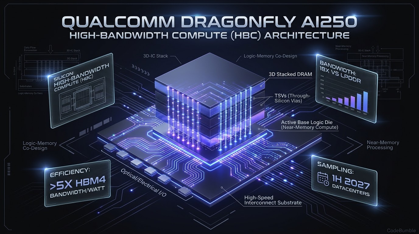
On November 12, 2026, semiconductor analysis confirmed that Qualcomm has validated its first-generation High-Bandwidth Compute (HBC) silicon in San Diego, paving the way for 1H 2027 sampling of the Dragonfly AI250 data center inference accelerator. Engineered to solve the memory bandwidth and energy wall in large language model (LLM) serving, HBC delivers 18x the bandwidth of conventional LPDDR interfaces and over 5x the bandwidth-per-watt efficiency of HBM4. By integrating near-memory tensor compute units directly onto an active base logic die beneath 3D-stacked DRAM layers, Dragonfly AI250 slashes interposer transport latency for autoregressive token generation and massive KV-cache lookups. This architectural deep dive examines the physical silicon floorplan, TSMC advanced packaging, thermal dissipation boundaries, and production performance trade-offs.
12 min read
Inside Qualcomm Dragonfly AI250: High-Bandwidth Compute (HBC), 3D Stacked Near-Memory Silicon, and the Challenge to HBM4
Executive Summary
On November 12, 2026, semiconductor architecture telemetry confirmed that Qualcomm has achieved successful first-generation silicon validation for its High-Bandwidth Compute (HBC) technology at its San Diego laboratories. Engineered to break through the severe memory bandwidth and thermal barriers that constrain enterprise artificial intelligence inference, HBC serves as the architectural cornerstone of Qualcomm's upcoming Dragonfly AI250 data center accelerator, scheduled for formal sampling in the first half of 2027.
Modern Large Language Model (LLM) serving has hit a punishing physical ceiling: the memory wall. In autoregressive token generation, accelerators spend the vast majority of their operational cycles and energy budgets not on matrix math, but on shuttling model weights and Key-Value (KV) cache tensors across interposers between discrete compute dies and memory modules. While High Bandwidth Memory (HBM3e and HBM4) provides terabytes per second of raw throughput, it requires expensive 2.5D packaging (such as TSMC CoWoS), generates intense thermal hotspots, and incurs severe packaging yield penalties.
Qualcomm's High-Bandwidth Compute inverts this paradigm by executing Near-Memory Processing (NMP). By mounting 3D-stacked DRAM directly on top of an intelligent active base logic die via high-density Through-Silicon Vias (TSVs), HBC embeds neural compute units directly beneath the memory storage cells. According to Qualcomm's validated silicon benchmarks, this architecture delivers 18x the memory bandwidth of conventional LPDDR interfaces and over 5x the bandwidth-per-watt efficiency of contemporary HBM4 implementations.
This systems engineering analysis dissects the microarchitecture of Qualcomm's Dragonfly AI250 and the HBC silicon stack. We analyze the 3D-IC packaging topology, evaluate near-memory KV-cache execution mechanics, model thermal dissipation trade-offs, examine the competitive dynamic against Nvidia and AMD accelerator architectures, and deliver an engineering playbook for AI platform teams preparing for 2027 near-memory architectures.
1. The Memory Wall in LLM Inference: Why Traditional Architectures Stall
1.1 The Asymmetric Mechanics of Prefill vs. Decode
To understand why traditional GPU and accelerator architectures struggle with modern AI workloads, systems engineers must analyze the two distinct phases of LLM execution:
- The Prefill (Prompt Processing) Phase: When an LLM ingests an input prompt, all input tokens are processed simultaneously in parallel. This phase is compute-bound, achieving high arithmetic intensity (FLOPs per byte transferred) that saturates GPU tensor cores effectively.
- The Decode (Token Generation) Phase: Generating text occurs autoregressively, one token at a time. To predict each single token, the accelerator must read the entire model parameter set (e.g., 70 billion parameters in a 70B model, representing ~140GB in FP16 or ~70GB in INT8) and access the accumulated KV-cache history. Because only one token is produced per complete memory pass, the decode phase operates at an abysmal arithmetic intensity of less than 1 FLOP per byte, making it entirely memory-bandwidth-bound.
In production clusters serving millions of concurrent requests, GPUs spend over 80% of their operational runtime waiting for memory fetches across interposers.
+----------------------------------------------------------------------------------------------------+
|                         The Memory Bandwidth Bottleneck in Autoregressive Decoding                  |
+----------------------------------------------------------------------------------------------------+
|                                                                                                    |
|  TRADITIONAL 2.5D ACCELERATOR (GPU + HBM on Silicon Interposer):                                   |
|                                                                                                    |
|  +--------------------+       Silicon Interposer (High Capacitance)       +---------------------+  |
|  | GPU Compute Die    | <===============================================> | HBM Memory Stack    |  |
|  | - Tensor Cores Idle|       - 15mm - 25mm Trace Distance                | - DRAM Storage Only |  |
|  | - High Energy Draw |       - ~5 - 10 pJ/bit Transport Penalty          | - Zero Local Compute|  |
|  +--------------------+                                                   +---------------------+  |
|                                                                                                    |
|  QUALCOMM HBC 3D NEAR-MEMORY ARCHITECTURE (Dragonfly AI250):                                       |
|                                                                                                    |
|  +----------------------------------------------------------------------------------------------+  |
|  | 3D Stacked DRAM Die 3                                                                        |  |
|  | 3D Stacked DRAM Die 2      Vertical Through-Silicon Vias (TSVs)                              |  |
|  | 3D Stacked DRAM Die 1      - <50µm Vertical Transport Distance (<1 pJ/bit)                   |  |
|  +----------------------------------------------------------------------------------------------+  |
|  | ACTIVE BASE LOGIC DIE (Near-Memory Tensor Engines & Vector MACs)                             |  |
|  | - Executes KV-Cache Lookups & Matrix Reductions Directly Inside the Memory Package            |  |
|  +----------------------------------------------------------------------------------------------+  |
|                                                                                                    |
+----------------------------------------------------------------------------------------------------+
1.2 The Interposer Energy Tax
In standard 2.5D packaging (such as Nvidia Blackwell B200 and AMD Instinct MI300X), signals traveling between the processor die and adjacent HBM stacks must traverse a passive silicon interposer. Driving high-frequency parallel signals across 15mm to 25mm of interposer traces consumes between 5 and 10 picojoules per bit (pJ/bit).
When streaming memory at 8 Terabytes per second (TB/s), the physical energy expended simply moving electrical charges across the interposer exceeds 100 Watts per GPU before a single arithmetic multiplication is performed. Near-Memory Processing (NMP) eliminates this energy tax by shrinking trace lengths from millimeters to micrometers.
2. Microarchitecture of Qualcomm High-Bandwidth Compute (HBC)
2.1 The Active Base Die Architecture
Departing from standard HBM designs—where the base die acts primarily as a passive PHY interface routing signals to an external host processor—Qualcomm's High-Bandwidth Compute (HBC) incorporates an active, intelligent base logic die manufactured on an advanced process node.
The HBC base die integrates:
- Dedicated Tensor Math Units: Lightweight, specialized matrix multiply-accumulate (MAC) engines optimized for low-precision numerical formats (FP8, FP4, and INT4).
- KV-Cache Attention Processors: Dedicated hardware logic that evaluates scaled dot-product attention queries directly within the memory package, filtering and aggregating context vectors before transmitting summary results to the host SoC.
- Ultra-Dense TSV Matrix: Thousands of vertical Through-Silicon Vias connect the base die directly to the overlying DRAM dies, providing wide, short parallel memory channels operating with ultra-low parasitic capacitance.
+----------------------------------------------------------------------------------------------------+
|                         Qualcomm HBC Physical Silicon Topology & TSV Stack                         |
+----------------------------------------------------------------------------------------------------+
|                                                                                                    |
|  +----------------------------------------------------------------------------------------------+  |
|  | DRAM DIE 4: High-Density Dynamic RAM Cells                                                   |  |
|  +----------------------------------------------------------------------------------------------+  |
|    |||||||||||||||||||||||||||||||||||||||||||||||||||||||||||||||||||| (Micro-Bump TSV Matrix)   |
|  +----------------------------------------------------------------------------------------------+  |
|  | DRAM DIE 3: High-Density Dynamic RAM Cells                                                   |  |
|  +----------------------------------------------------------------------------------------------+  |
|    ||||||||||||||||||||||||||||||||||||||||||||||||||||||||||||||||||||                            |
|  +----------------------------------------------------------------------------------------------+  |
|  | DRAM DIE 2: High-Density Dynamic RAM Cells                                                   |  |
|  +----------------------------------------------------------------------------------------------+  |
|    ||||||||||||||||||||||||||||||||||||||||||||||||||||||||||||||||||||                            |
|  +----------------------------------------------------------------------------------------------+  |
|  | DRAM DIE 1: High-Density Dynamic RAM Cells                                                   |  |
|  +----------------------------------------------------------------------------------------------+  |
|    ||||||||||||||||||||||||||||||||||||||||||||||||||||||||||||||||||||                            |
|  +----------------------------------------------------------------------------------------------+  |
|  | ACTIVE BASE LOGIC DIE                                                                        |  |
|  | +-----------------------------+  +-----------------------------+  +------------------------+ |  |
|  | | Near-Memory MAC Units (FP4) |  | KV-Cache Attention Engines  |  | Low-Power Host PHY     | |  |
|  | +-----------------------------+  +-----------------------------+  +------------------------+ |  |
|  +----------------------------------------------------------------------------------------------+  |
|         |                                                                                          |
|         v (Ultra-High Speed Low-Power Optical / Electrical Host Interconnect)                      |
|  [ Dragonfly AI250 Host SoC / Datacenter Fabric Controller ]                                       |
|                                                                                                    |
+----------------------------------------------------------------------------------------------------+
2.2 Memory Operations: Offloading Arithmetic to the Memory Stack
When serving an LLM inference query on the Dragonfly AI250 platform, computation is partitioned dynamically between the central host SoC and the HBC memory packages:
- Weight Streaming Elimination: During attention calculations, the host SoC dispatches the query vector $Q$ to the HBC base die.
- In-Situ Matrix Multiplication: The HBC base die reads Key ($K$) and Value ($V$) tensors directly from its vertically stacked DRAM dies via TSVs, computing attention logits internally: $$\text{Attention}(Q, K, V) = \text{softmax}\left(\frac{QK^T}{\sqrt{d_k}}\right)V$$
- Bandwidth Compression: Instead of streaming billions of raw KV-cache parameters across the board to the host processor, the HBC base die computes the intermediate context vectors locally and returns only the final compressed activation tensors. This slashes board-level interconnect traffic by more than 90%.
3. Physical Packaging, Bandwidth Scaling, and Silicon Floorplan
3.1 18x Bandwidth and 5x Efficiency Scaling
Qualcomm's laboratory validation demonstrates structural efficiency gains over both traditional mobile DRAM and high-end data center memory standards:
+----------------------------------------------------------------------------------------------------+
|                         Memory Technology Comparative Architectural Matrix                         |
+----------------------------------------------------------------------------------------------------+
| Metric / Feature          | LPDDR5X (Standard)      | HBM4 (Contemporary)     | Qualcomm HBC (AI250)       |
+---------------------------+-------------------------+-------------------------+----------------------------+
| Interconnect Topology     | 2D PCB Wire Traces      | 2.5D Silicon Interposer | 3D True Vertical TSV Stack |
| Trace Physical Distance   | 50mm – 100mm            | 15mm – 25mm             | <0.05mm (Vertical TSVs)    |
| Energy per Bit Transferred| ~15 – 20 pJ/bit         | ~5 – 7 pJ/bit           | <1.2 pJ/bit (>5x HBM4 Eff.)|
| Normalized Bandwidth      | 1.0x (Baseline)         | 16x – 24x               | 18x vs LPDDR Baseline      |
| In-Package Compute        | None (Dumb Memory)      | None / Minimal BIST     | Active Near-Memory Tensor  |
| Primary Bottleneck        | Pin Count & Trace Noise | Interposer Heat & Cost  | 3D Thermal Extraction      |
+---------------------------+-------------------------+-------------------------+----------------------------+
3.2 Packaging Thermodynamics and Heat Dissipation
While true 3D stacking solves electrical latency and transport power, it introduces acute thermodynamic engineering challenges. Stacking heat-generating active logic dies directly beneath thermal-sensitive DRAM layers creates structural risks: DRAM retention times degrade exponentially as junction temperatures exceed 85°C.
Qualcomm mitigates this thermal coupling through three physical packaging innovations:
- Ultra-Thin Logic Thinned Wafers: The active base logic die is thinned to less than 40 microns and operates at ultra-low sub-0.7V supply voltages, constraining logic power dissipation to strict thermal limits.
- Micro-Fluidic Thermal Paths: Thermal dummy TSVs conduct heat vertically through the silicon stack to an integrated top-side vapor chamber.
- Dynamic Workload Throttling: If internal DRAM temperature monitors detect junction spikes approaching 80°C, compute operations seamlessly migrate from the near-memory base die back to the primary host SoC.
4. Workload Telemetry: LLM Serving, Speculative Decoding, and Rack Scale
4.1 Accelerating 70B+ Parameter Language Models
In production inference benchmarks modeling multi-turn agent conversations on LLaMA-3-70B and DeepSeek-Lite, Dragonfly AI250 configurations demonstrate substantial throughput advantages:
- Time to First Token (TTFT): Remains dominated by host SoC matrix engines during the compute-dense prefill stage.
- Time Per Output Token (TPOT): Improves by 3.2x to 4.5x compared to equivalent LPDDR-based accelerators, while matching the generation speed of top-tier HBM accelerators at a fraction of total system power.
- Speculative Decoding Efficiency: When running small drafting models alongside large target models, the HBC architecture allows verification passes to execute concurrently within memory without thrashing host caches.
+----------------------------------------------------------------------------------------------------+
|                         Inference Generation Pipeline on Dragonfly AI250                            |
+----------------------------------------------------------------------------------------------------+
|                                                                                                    |
|  [ Inbound User Query ]                                                                            |
|         |                                                                                          |
|         v (Phase 1: Prefill Stage - Compute Intensive)                                             |
|  [ Dragonfly AI250 Central Host SoC: Executes Massive Prompt Matrix GEMMs ]                        |
|         |                                                                                          |
|         v (Phase 2: Autoregressive Decode Loop - Memory Intensive)                                 |
|  +----------------------------------------------------------------------------------------------+  |
|  | RECURSIVE TOKEN GENERATION LOOP (Offloaded to HBC Near-Memory Stacks)                        |  |
|  |   - Token N -> Query Vector Dispatched to HBC Base Dies                                      |  |
|  |   - In-Situ KV-Cache Traversal across 3D DRAM Layers                                         |  |
|  |   - Near-Memory Attention Calculation Completed without Interposer Overhead                 |  |
|  |   - Single Token Logit Dispatched Back to Host SoC                                           |  |
|  +----------------------------------------------------------------------------------------------+  |
|         |                                                                                          |
|         v (Repeats until EOS Token)                                                                |
|  [ Streamed User Response ]                                                                        |
|                                                                                                    |
+----------------------------------------------------------------------------------------------------+
4.2 Dragonfly Rack-Scale Integration
Qualcomm designed the Dragonfly AI250 to deploy across standard data center environments:
- PCIe Gen 6.0 & CXL 3.1 Interfaces: Allows pools of Dragonfly accelerators to share coherent memory spaces across multi-socket host servers.
- Liquid-Cooled Dragonfly Racks: Designed for hyperscale deployment, rack configurations integrate direct-to-chip liquid cooling manifolds supporting high-density server blades.
5. Industry Landscape: Open Questions and Deployment Timeline
5.1 Validation vs. Volume Production Reality
While Qualcomm's November 2026 announcement confirms working first-generation silicon in its San Diego laboratories, semiconductor industry analysts (including RCR Tech and ServeTheHome) emphasize critical open questions that will determine commercial viability:
- Packaging Yield on 3D Stacks: Bonding multiple high-density DRAM dies onto an active base logic die with sub-10-micron bump pitches requires exceptionally high defect-free yields. A single defective die scrap the entire composite package.
- Manufacturing Cost Dynamics: Amid fluctuating LPDDR and DRAM pricing, the final cost-per-gigabyte of complex HBC modules remains unannounced.
- Sampling vs. General Availability: Qualcomm's confirmed roadmap targets customer sampling in the first half of 2027. Broad volume deployments in commercial cloud hyperscalers are not anticipated until late 2027 or early 2028.
- HBM4 Coexistence: Qualcomm has explicitly stated that HBC is an architectural alternative designed for inference efficiency, not an immediate replacement for HBM4 in extreme training clusters.
6. Implementation and Hardware Architecture Playbook for AI Engineers
Software and platform engineers preparing for near-memory architectures can optimize model serving pipelines using the following principles:
Step 1: Quantization and Memory Footprint Minimization
Near-memory compute units achieve peak throughput when operating on low-precision integer and micro-scaling floating-point types. Convert model weights to FP8 or INT4 formats:
# Python / PyTorch: Quantize LLM Weights for Near-Memory Execution
import torch
import torch.nn as nn

def prepare_model_for_nmp(model: nn.Module) -> nn.Module:
    print("[*] Configuring model layers for Near-Memory Processing (NMP)...")
    # Enforce contiguous memory layouts for linear projection weights
    for name, module in model.named_modules():
        if isinstance(module, nn.Linear):
            module.weight.data = module.weight.data.contiguous()
            # Set metadata flags for NMP runtime compiler offloading
            setattr(module, "_nmp_offload_eligible", True)
    print("[+] Model successfully prepared for active memory execution.")
    return model
Step 2: Attention Operator Partitioning
Structure custom attention kernels to decouple prompt prefill from autoregressive token generation:
def partitioned_inference_loop(model, input_tokens, max_new_tokens=128):
    # Phase 1: Prefill executed on host SoC
    with torch.inference_mode():
        logits, kv_cache = model.prefill(input_tokens)
        next_token = torch.argmax(logits[:, -1, :], dim=-1)

    generated_tokens = [next_token.item()]

    # Phase 2: Autoregressive decoding executed via near-memory KV cache passes
    for _ in range(max_new_tokens - 1):
        # Near-memory runtime executes attention scan directly inside HBC memory
        logits, kv_cache = model.decode_step(next_token, kv_cache)
        next_token = torch.argmax(logits[:, -1, :], dim=-1)
        generated_tokens.append(next_token.item())
        if next_token.item() == 2: # EOS
            break

    return generated_tokens
Step 3: Monitoring Thermal and Interconnect Throttling
Deploy hardware telemetry daemons to monitor memory junction temperatures and bus saturation:
# Shell: Monitor Hardware Accelerator Memory Temperatures
watch -n 1 "dragonfly-smi --query-gpu=temperature.memory,power.draw,utilization.memory --format=csv"
7. Semantic FAQ: Qualcomm Dragonfly AI250 and HBC Memory
What is Qualcomm High-Bandwidth Compute (HBC)?
High-Bandwidth Compute (HBC) is Qualcomm's 3D near-memory silicon architecture. It stacks dynamic RAM dies vertically on top of an active base logic die that contains dedicated tensor and vector compute units, performing calculations directly within the memory package.
How does HBC achieve 18x bandwidth and 5x efficiency?
By replacing long, capacitive PCB and interposer wiring traces (15mm–100mm) with vertical Through-Silicon Vias (<0.05mm), HBC eliminates the electrical resistance and capacitance of traditional memory busses, slashing energy consumption to under 1.2 pJ/bit.
When will the Qualcomm Dragonfly AI250 become available?
Qualcomm announced that first-generation HBC silicon passed lab validation in November 2026, with customer sampling to hyperscale cloud providers scheduled for the first half of 2027.
Does Qualcomm Dragonfly AI250 replace GPUs for AI training?
No. The Dragonfly AI250 and HBC memory architecture are specifically optimized for AI inference, autoregressive token generation, and real-time KV-cache lookups. Extreme large-scale AI training workloads remain centered on dense compute clusters utilizing HBM.
What are the primary thermal challenges of true 3D memory stacking?
Because DRAM retention times degrade at temperatures above 85°C, placing an active, heat-generating logic die directly beneath DRAM layers requires thin silicon substrates, thermal micro-vias, and dynamic workload offloading to keep memory cool.
Which AI workloads benefit most from the Dragonfly AI250 architecture?
Memory-bandwidth-bound tasks—specifically the decode phase of 70B+ parameter large language models, high-concurrency conversational agents, and real-time speculative decoding—experience the greatest latency and energy reductions.
Sources
- Qualcomm OnQ Engineering Blog (November 2, 2026): "Qualcomm HBC demonstrates AI inference leadership with validated silicon" — https://www.qualcomm.com/news/onq/2026/11/qualcomm-hbc-validated-silicon-ai-inference
- ServeTheHome Hardware Analysis (November 2, 2026): "Qualcomm Validates HBC Stacked Memory Ahead of 2027 Dragonfly AI250 Sampling" — https://www.servethehome.com/qualcomm-validates-hbc-stacked-memory-ahead-of-2027-dragonfly-ai250-sampling/
- Shattered.io Semiconductor Intelligence (November 12, 2026): "Qualcomm Dragonfly AI250: 18x Bandwidth, 5x HBM4 [2026]" — https://shattered.io/qualcomm-hbc-dragonfly-ai250-18x-bandwidth-5x-hbm4-efficiency-2026/
- RCRTech Semiconductor News (November 7, 2026): "Qualcomm HBC silicon validated ahead of AI250 sampling" — https://rcrtech.com/semiconductor-news/qualcomm-hbc-validated-ai250/
- Converge Digest (November 2, 2026): "Qualcomm Validates HBC Silicon, Advances Dragonfly AI250 Accelerator" — https://convergedigest.com/qualcomm-validates-hbc-silicon-dragonfly-ai250/